Electrick: making a touchpad out of nearly anything

Nowadays, most people will have a smartphone, a tablet, or perhaps even a touch sensitive television. What all of these screens have in common, however, is that they are relatively small and flat. Future Interfaces Group, an interdisciplinary research lab within the Carnegie Mellon University, shows in a project called Electrick that it is possible to make a touchpad out of nearly anything, big or small, flat or irregular, using a variety of conductive materials.
The project is described as “a low-cost and versatile sensing technique that enables tough input on a wide variety of objects and surfaces”. To make the surfaces, they combine an electric field tomography with an electrically conductive material.
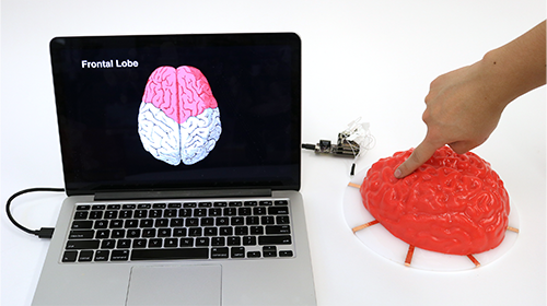
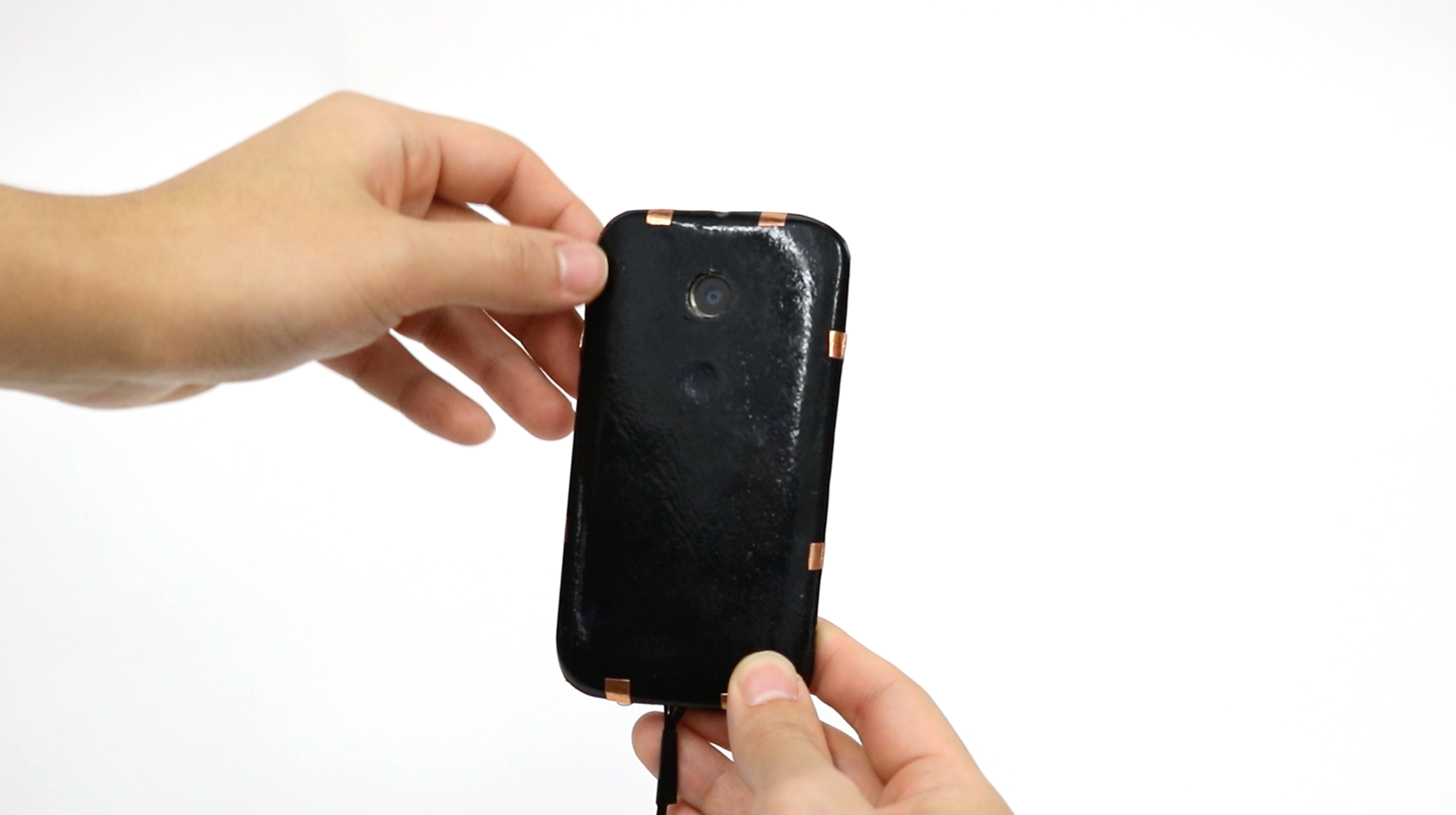
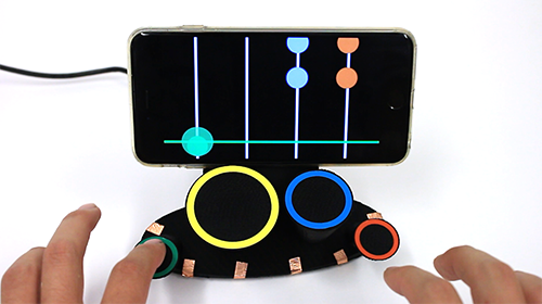
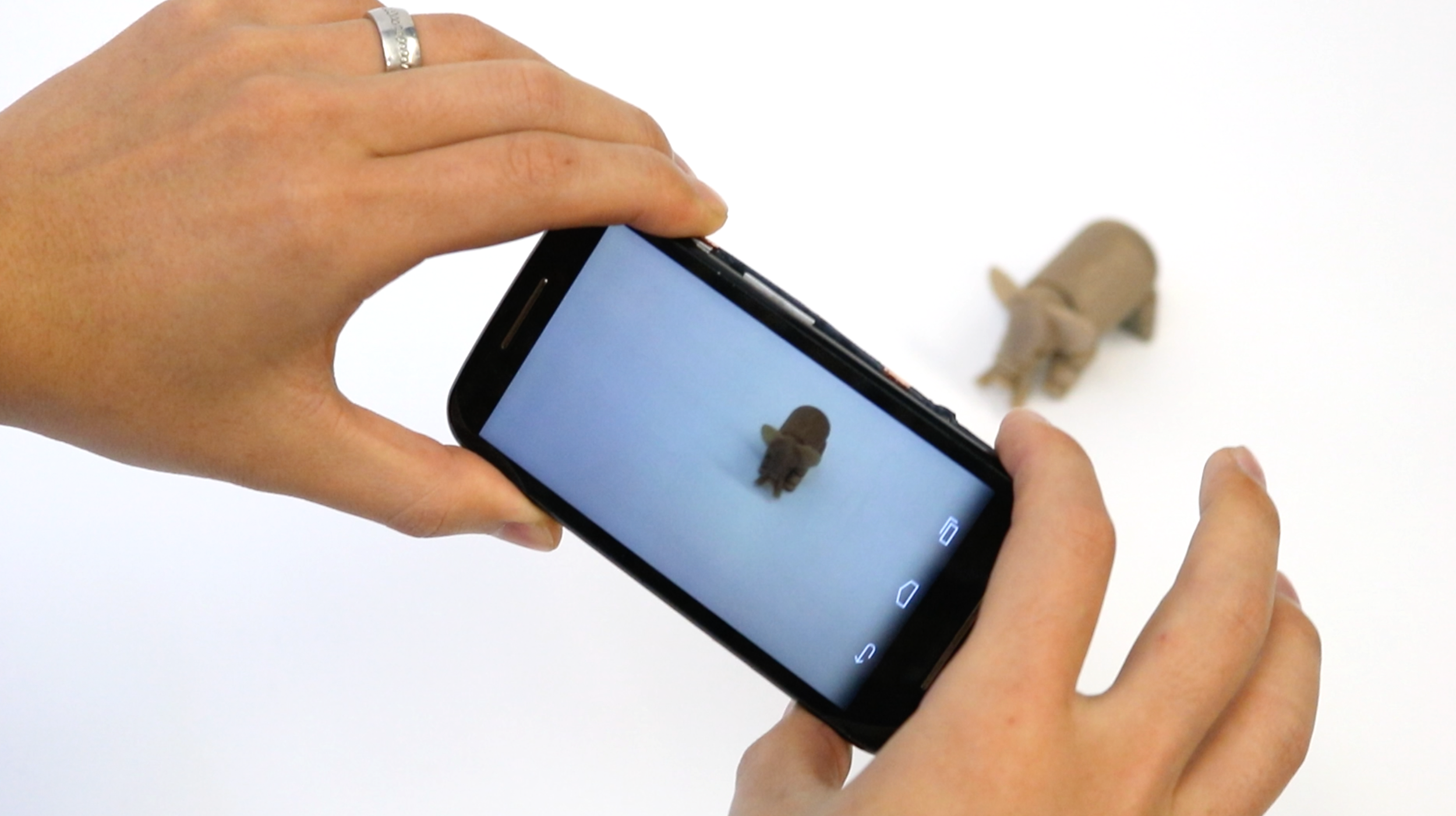
The sensing principle works by injecting a small electrical current into the conductive layer, using a pair of electrodes. The voltage is measured by all adjacent voltage points. When a finger touches the surface, some power is shunted, causing a localised reduction in voltage. By rotating the place the electrical current is coming from, an estimate can be made where the surface is touched, using tomographic reconstruction. With standard blob-tracking techniques, finger locations and movements can be tracked on a computer screen.
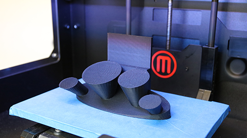
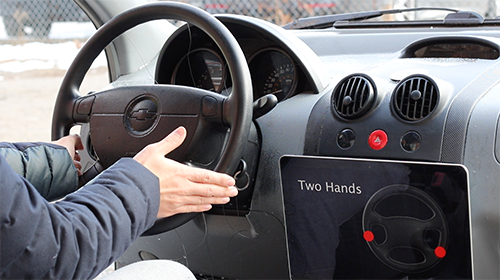
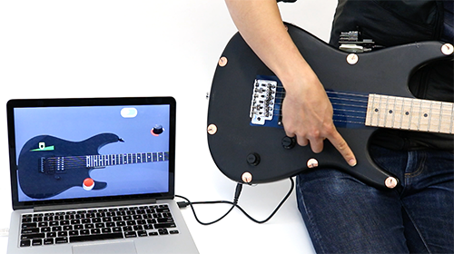
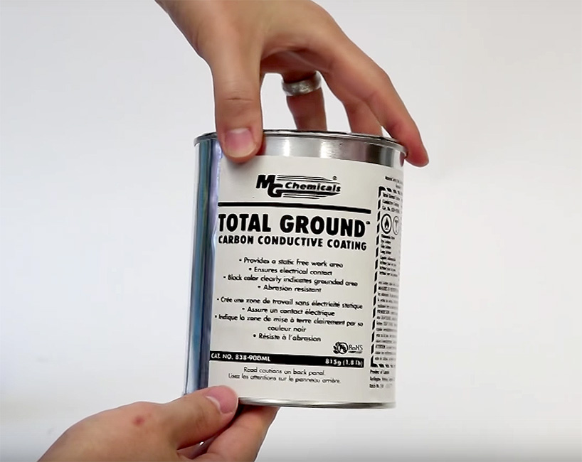
The group used various materials to demonstrate the technique. As example they mention Velostat, which is a carbon-loaded polyolefin film that can be attached to surfaces with adhesives to make inexpensive touchpads. Carbon-loaded ABS, sold as filament, can also be used to create conductive objects. Using a conductive paint, almost anything can be turned into a touchpad, no matter how big or irregular. The team demonstrates that even entire walls can be used as touchpads, as well as shapes made from Jell-O and Play-Doh.
Electrick shows that nearly any object can be ‘smart’ and interactive if it is made from or covered in a conductive material, once it is hooked up to electrodes and a computer. Watch the video below to see a whole range of examples and the materials in action.
Photos: Carnegie Mellon University

Comments